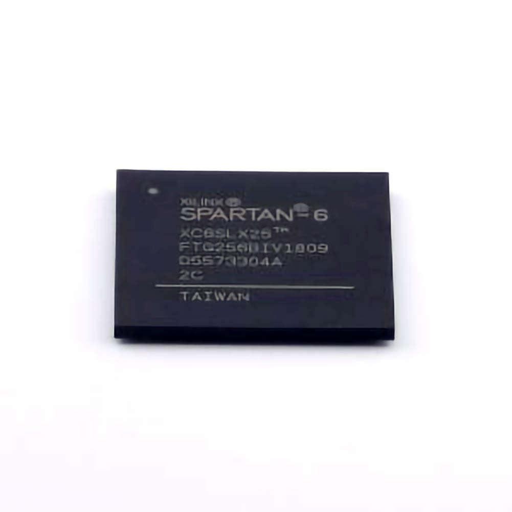
This article provides a detailed overview of common troubleshooting techniques and solutions for the XC6SLX25-2FTG256C FPGA . Designed for engineers and developers, it covers key issues and practical solutions for optimizing the functionality and performance of this versatile FPGA device.
XC6SLX25-2FTG256C, troubleshooting, FPGA, solutions, common issues, Electrical problems, configuration, signal integrity, performance optimization, Xilinx, circuit design, debugging
Introduction to the XC6SLX25-2FTG256C FPGA
The XC6SLX25-2FTG256C is part of Xilinx's Spartan-6 series, offering an impressive blend of performance and flexibility for a wide range of applications. With 25,000 logic cells, it is capable of handling a variety of complex designs, from simple signal processing tasks to sophisticated embedded systems. However, like any high-performance FPGA, the XC6SLX25-2FTG256C can encounter specific challenges in the development cycle.
Whether you are designing a new circuit, debugging a problem, or optimizing an existing implementation, it’s important to understand the common issues that can arise during the lifecycle of the XC6SLX25-2FTG256C. This guide will address some of the most frequently encountered problems and provide effective troubleshooting strategies.
1. Power Supply Issues
One of the most common causes of malfunction in FPGAs, including the XC6SLX25-2FTG256C, is an improper power supply. FPGA devices are sensitive to voltage fluctuations and current supply quality. The Spartan-6 series requires multiple voltage rails, typically 3.3V for I/O and 1.2V or 2.5V for core voltage.
Common Symptoms:
Device not powering on.
Unstable operation or random resets.
Communication failures with external components.
Troubleshooting Solutions:
Check Voltage Levels: Ensure that the power supply delivers the correct voltage levels at the specified tolerance ranges. A common error is failing to check the tolerance levels for each power rail. Use a multimeter or oscilloscope to confirm stable voltage during power-up.
Current Requirements: Verify that your power supply can provide the necessary current without dipping below recommended levels. Insufficient current can lead to performance degradation or failure to start up correctly.
Decoupling Capacitors : Use the recommended decoupling capacitors near the power pins to reduce noise and voltage spikes.
Power Sequencing: Spartan-6 FPGAs require proper power-up sequencing. Ensure that the core and I/O voltages are powered up in the correct sequence to avoid device damage.
2. Configuration Failures
After ensuring a stable power supply, the next common issue is configuration failure. The XC6SLX25-2FTG256C supports various configuration methods, including JTAG, SPI, and BPI, but misconfiguration can lead to system failures.
Common Symptoms:
The device fails to load the bitstream.
Configuration errors during boot-up.
Incorrect functionality after configuration.
Troubleshooting Solutions:
Verify Bitstream Integrity: The first step is to confirm that the bitstream file is not corrupted. Ensure that the file was correctly generated in your FPGA design tool (e.g., Vivado) and that it is compatible with the specific FPGA model and package.
Check Configuration Mode: Ensure the FPGA is set to the correct configuration mode (e.g., JTAG, Master SPI, or Parallel). Using the wrong configuration mode can prevent the FPGA from loading the bitstream properly.
Inspect Configuration Pins: Check the configuration pins (like M0, M1, etc.) to ensure they are correctly set for the desired configuration method. Incorrect pin connections or floating pins could cause configuration issues.
Reprogramming: If the FPGA fails to configure properly, attempt to reprogram the device using the preferred programming method, and ensure there is no electrical noise or interference during this process.
3. Signal Integrity Problems
Signal integrity problems can significantly affect the performance of the XC6SLX25-2FTG256C FPGA, especially in high-speed applications. These problems often manifest as unreliable signals, slow performance, or logic errors in the FPGA.
Common Symptoms:
Unstable or noisy signals.
Slow or erratic performance.
Random or incorrect outputs.
Troubleshooting Solutions:
PCB Layout and Routing: Poor PCB layout and routing are frequent culprits of signal integrity issues. Ensure that high-speed signals are routed properly, with minimal length, and avoid unnecessary vias. Use differential pair routing for high-speed signals like Clock lines.
Termination Resistors : Proper termination of signal lines is critical. Use series resistors, pull-up/down resistors, or appropriate termination networks for high-speed lines, particularly when dealing with high-frequency clock signals.
Ground Planes: A solid, continuous ground plane can reduce noise and improve the overall signal integrity. Avoid breaks or gaps in the ground plane under high-speed traces.
Use of Buffers and Drivers : Use buffers or line drivers for long traces or when driving multiple components from a single output. This can help maintain signal strength and reduce the possibility of signal degradation.
4. Clock Issues and Timing Violations
Clocks are essential for FPGA operation, and timing violations or clock issues are among the most frustrating challenges engineers face when working with devices like the XC6SLX25-2FTG256C. Clock-related problems can arise from improper clock sources, clock jitter, or timing violations in your design.
Common Symptoms:
Incorrect or unstable outputs.
Timing violations in the design.
High jitter or clock instability.
Troubleshooting Solutions:
Clock Source Quality: Ensure that the clock source feeding the FPGA is clean and stable. High jitter or noise on the clock line can cause timing issues. Use a low-jitter oscillator or crystal if necessary.
Clock Distribution Network: Review your clock distribution network to ensure that the clock is routed properly and distributed evenly across the FPGA.
Timing Analysis: Use the FPGA’s built-in timing analysis tools (like Vivado’s Timing Analyzer) to check for setup and hold time violations. If violations are detected, adjust your design or increase the timing margins by modifying the clock constraints.
5. Thermal Management Problems
FPGAs, including the XC6SLX25-2FTG256C, can generate significant heat, especially under heavy load. Inadequate thermal management can lead to overheating, which may cause the FPGA to shut down or operate erratically.
Common Symptoms:
FPGA overheating or thermal shutdown.
Performance degradation.
Erratic behavior under load.
Troubleshooting Solutions:
Thermal Monitoring: Ensure that the FPGA is operating within its thermal limits by monitoring the device temperature. Use an infrared thermometer or a dedicated thermal sensor to check the surface temperature.
Heat Sinks and Cooling: In designs with high power consumption or dense logic, consider adding heat sinks or improving airflow to keep the FPGA within safe operating temperatures.
Power Dissipation: Optimize the design to minimize power consumption where possible. Use clock gating, reduce unnecessary logic usage, and power down unused parts of the FPGA to reduce heat generation.
Advanced Troubleshooting and Performance Optimization for XC6SLX25-2FTG256C
6. I/O Pin and Signal Configuration Issues
The XC6SLX25-2FTG256C provides a versatile set of I/O pins that can be configured for different voltage levels and signal types. Incorrect configuration of these I/O pins can lead to electrical conflicts, signal integrity issues, or even permanent damage to the FPGA.
Common Symptoms:
Unresponsive or incorrectly functioning I/O.
Signal conflicts or short circuits.
Electrical damage to the I/O pins.
Troubleshooting Solutions:
I/O Voltage Levels: Ensure that the voltage levels for the I/O pins match the specifications in the datasheet. Mismatched voltage levels can cause permanent damage to the FPGA or connected peripherals.
I/O Standards: Configure the I/O pins for the correct I/O standard (LVCMOS, LVDS, etc.) based on the external devices they are connected to. The wrong I/O standard can result in unreliable communication or signal corruption.
Pin Assignment: Review the pin assignment in your design. Incorrect assignments can result in incorrect functionality or conflicts with other components in the system.
Use I/O Buffers: If driving high-speed signals or long traces, use I/O buffers to ensure the signal maintains integrity across the PCB.
7. Design Logic Errors and Debugging
Another source of issues in FPGA systems is logic errors within the design itself. These errors may not be immediately apparent but can lead to incorrect behavior once the FPGA is configured.
Common Symptoms:
Incorrect outputs or functionality.
Logic fails to match the intended behavior.
Unpredictable results in simulation versus actual hardware.
Troubleshooting Solutions:
Simulation: Always simulate your design using tools like Vivado's simulation features before deploying it to the hardware. This can catch a wide range of logic errors before you program the FPGA.
On-Chip Debugging: Xilinx provides various debugging tools, such as the Integrated Logic Analyzer (ILA), which can help you capture real-time signals inside the FPGA. Use the ILA to monitor signal transitions and internal states.
Design Constraints: Double-check your constraints files for any mismatched timing, I/O assignments, or placement constraints that may cause issues at runtime.
8. Overcoming Clock Domain Crossing (CDC) Issues
When your FPGA design includes multiple clock domains, clock domain crossing (CDC) can introduce synchronization issues and lead to data corruption or timing errors.
Common Symptoms:
Incorrect data transfers between clock domains.
Data loss or corruption in the design.
Timing errors when crossing domains.
Troubleshooting Solutions:
Use FIFO Buffers: One of the most common solutions to CDC issues is using FIFO buffers to ensure that data is transferred safely between clock domains without violating timing constraints.
Gray Code Encoding: Implement Gray Code for state machines crossing clock domains to avoid race conditions.
CDC Tools: Use Vivado’s CDC analyzer to detect potential issues between clock domains and optimize your design accordingly.
9. Resource Utilization and Performance Optimization
As your design becomes more complex, resource utilization (logic cells, memory, etc.) increases, which can impact performance. Optimizing resource usage ensures that your design can run at maximum efficiency.
Common Symptoms:
The design is too large to fit into the available logic cells.
Performance bottlenecks due to inefficient resource use.
Troubleshooting Solutions:
Resource Constraints: If you’re running out of resources, consider reducing the number of logic cells used or using smaller, more efficient functions. Reevaluate your design to minimize resource demand.
Performance Profiling: Use Vivado’s performance profiling tools to identify bottlenecks in your design. This can help pinpoint areas where optimization is needed.
10. External Component Compatibility
In many applications, the XC6SLX25-2FTG256C interacts with external components like sensors, memory, or communication module s. Compatibility issues can arise from mismatched voltage levels, communication protocols, or timing constraints.
Common Symptoms:
Communication failures with external devices.
Data corruption or synchronization errors.
Hardware damage from voltage mismatches.
Troubleshooting Solutions:
Voltage Level Translation: If communicating with devices that use different voltage levels, use level shifters to match voltage requirements.
Protocol Mismatches: Ensure that the communication protocol (I2C, SPI, UART, etc.) matches on both ends. Double-check baud rates, data formats, and signal connections.
Conclusion
Troubleshooting the XC6SLX25-2FTG256C FPGA involves a systematic approach to identify the underlying issues, whether related to power supply, configuration, signal integrity, or logic design. By understanding the common problems and their solutions, you can significantly improve the reliability and performance of your FPGA-based projects. By carefully following the guidance outlined in this article, you will be equipped to handle any challenges that arise during the development or deployment of your Spartan-6 FPGA designs.
If you are looking for more information on commonly used Electronic Components Models or about Electronic Components Product Catalog datasheets, compile all purchasing and CAD information into one place.
Partnering with an electronic components supplier sets your team up for success, ensuring the design, production, and procurement processes are quality and error-free.


